


 APU, Fusion, Vision, IGP, heterogeneously programmable chip. High degree of integration. All in one tile. These are the keywords. Available is Llano, which fights for the favors of customers on both desktop and mobile platforms. After the AMD A8-3850 APU, the A6-3650 also visited us…
This story started about 5 years ago. We all got our heads up when we heard the news when AMD announced its acquisition of ATI Technologies, which was famous for its Radeon branded video cards and motherboard chipsets. At the time, the average person had a hard time understanding why this step was needed by the number two processor manufacturers, but there were many who could already read between the lines.
The GPU business wasn't the business of the millennium even then, and a significant portion of the Radeons found new homes in Intel machines, but part of that area had to be said to say goodbye under the AMD brand. AMD aimed this move more at the future than the present, which otherwise cost the company $ 5,4 billion. To do this required loans, huge repayment installments, a declining stake, an Intel advantage, and the economic crisis caused serious hardships in the company’s life. Despite all the difficulties, AMD had virtually no choice.
Leaders realized that in order to survive in the long run, it would be necessary to bring to life a complete, all-encompassing platform that Intel was already in full swing at the time. This means that the processor, the chipset, which may include a graphics core, and the graphics controllers must be built within their own walls under the same branding. That was the basic idea, but an even more forward-thinking idea was conceived in the minds of engineers, an idea called Fusion in baptism. This concept included that CPU and GPU tasks should be combined on a single slice of silicon. As the processor manufacturer did not have the technology and experience to produce GPUs, the acquisition of ATI proved to be an unavoidable step in this direction as well.
For a long time, very little was known about Fusion, but as time went on, more and more information dripped about upcoming products and technologies, while it was not until the first Fusion representative had to wait until February this year. This eventually became not the Llano, but the Brazos platform, with which AMD sent a serious message of war to the Intel Atom product line, and a bloody battle began in the field of nettops and netbooks, respectively.

So we could already get acquainted with the term APU in connection with Brazos, who would have fallen behind, we recommend our article on the subject. Half a year later, the sequel has arrived, with the release of Llano, APUs are also moving into more powerful desktop and mobile computers, let’s see what you need to know about the new family!

AMD has no secret of high hopes for Llano's chips. The novelty on the day of its release our colleague has already presented it in detail, but as the saying goes, “repetition is the mother of knowledge”.

What are “Llano,” “Lynx,” and “Sabine”?
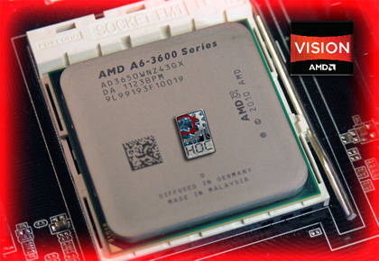
The new products of the second largest processor manufacturer are accompanied by several fancy names. The chip, codenamed Llano, is another heterogeneously programmable (Accelerated Processing Unit). The APU is made on GlobalFoundries ’32nm SHP production lines, has a physical area of 228 square millimeters and contains 1,45 billion transistors. The chip carries up to four x86 processor cores as well as a powerful IGP with 400 computing units. Llano can be seen as the foundation of two platforms: Lynx on the desktop and Sabine on the mobile market. The latter can pack system memory operating at up to 1600 MHz into the two SODIMM sockets, while the former can be official DDR1866 memory up to 3 MHz at 1,5 volts.

Members of the Sabine platform
Foreword is that AMD has hit the corner with Llano on its very head. Analysts expect a steady decline in the market for stand-alone GPUs - Fusion is now just oil on the fire - and meeting the needs of users requires such products. The APU has the performance of an Athlon II X4 or a low-end discrete graphics card, making it attractive to a very wide layer.

The full desktop Llano range
Every level, almost everything!
AMD A4 Series - The Entry Level
As a member of the A4 series, the A4-3400 includes a dual-core processor and an integrated Radeon HD 6410D graphics controller. The CPU is at 2,7 GHz and the graphics processor is at 600 MHz. The APU is in the 100 watt power class. The A4-3300 has similar parameters, unchanged SUMO controller with 160 computing units and 1 MB second level cache. The product was born with essentially a simple clock reduction, so the CPU speed was taken back by 200 MHz, while the GPU speed was taken back by 157 MHz.
AMD A6 Series - The Middle Class
The series has three members, but initially only that A6-3650 will be available. The quad-core processor is clocked at 2,6 GHz and consumes up to 100 watts. This is followed by the A6-3600 - 2,4 / 2,1GHz (Turbo Core), also equipped with four cores. It can be seen from the APU numbering (ending in xx00) that its power demand is below 65 watts. In the smallest copy, the engineers deactivated a processor core, but applied no other change compared to the A6-3600. All three APUs feature the HD 6530D, in which 320 shaders have been activated.

The tip of the iceberg: A8 and A6 series
AMD A8 Series - The Upper Housing


AMD A8-3850 APU top and bottom
The most powerful Lynx APUs can be found here. The category currently relies on two models, but the A8-3870 “Black Edition” will arrive later this year. The four processor cores of the A8-3850 run at 2,9 GHz, so it's no wonder the 100 Watt energy hunger. The A8-3800 – 2.7/2.4GHz (Turbo Core) – looks promising not only at first glance in terms of the consumption-performance indicator. The integrated GPU of the A8 series is the Radeon HD 6550D.


"Sumo" is unbeatable
Llano’s “Sumo” integrated graphics processor is a kind of Redwood reincarnation. The IGP was equipped with five 80-way shader arrays, 20 Gather4-compatible texturing channels, and two ROP blocks with eight blending units. The GPU, of course, uses system memory to store data, which the APU can access through the dual-channel memory controller. Envelope in advance, the performance of a controller that is buffalo in its category depends significantly on memory speed. Based on measurements from foreign test sites, it is advisable to use at least 1600MHz DDR3 memories, otherwise a significant slowdown can be expected. Like the Brazos platform, all vendor-independent technologies are supported: DirectX 11, OpenGL 4.1, OpenCL 1.1, OpenGL ES 2.0, WebGL, WebCL, DirectCompute 5.0.

And the UVD 3 media engine guarantees H.264 / AVC, MPEG-2/4, VC-1, DivX and Xvid video acceleration up to Ultra HD resolution. AMD saw fit to revive the Hybrid CrossFire concept, now called Dual Graphics. This means that discrete graphics cards defined next to the Llano IGP can be associated, adding up the speeds of the two. However, the function only works with a few controls, which are shown below. The PCI-E controller can handle a total of 24 bands, of which 16 are for an external video controller, 4 for the FCH, and four more for devices that require low latency and relatively high bandwidth, such as Ethernet.
Thank you, you can sit down, great.


The other side of the coin
The CPU cores, called the APU Husky, don’t have third-level cache, but engineers have increased the size of the L512 cache from 1 kilobytes to 2 megabyte, somewhat to make up for the shortfall. The cache size of L1 data and L1 instruction is 64-64 KB.

The structure of the architecture is very similar to the already obsolete K10 solutions. Each core consists of 35 million transistors, has an area of 9,7 mm2 and a typical consumption of 10-15 watts, which can be reduced to 2,5 watts when unloaded due to aggressive gating. The instruction sets include SSE1, SSE2, SSE3, SSE4A and all 3DNow! knows the extension. Given the history of the architecture, unsurprisingly, it does not support SSE 4.1 and 4.2.

The presence of TurboCore 2.0 is not a negligible factor. This feature even came with Thuban tiles. The method is able to greatly increase the clock speed of the processor cores only if the increased consumption does not exceed the maximum specified TDP limit. Using a specific example for ease of understanding: if the IGP is fully loaded, the CPU clock cannot be raised, but if only the UVD engine is loaded - which has negligible power consumption - TurboCore 2.0 can significantly increase the Husky core clock so that the increased consumption still fits within the predefined TDP frame. This can mean up to 35 MHz extra speed for 900-watt mobile versions. It’s also important to mention here that TurboCore 2.0 only applies to processor cores, not to IGP anymore.
Closely related to this is the improved energy management, which is now able to completely disconnect components that are not in use, thus significantly reducing chip consumption.


