


 APU, Fusion, Vision, IGP, heterogeneously programmable chip. High degree of integration. All in one tile. These are the keywords. Available is Llano, which fights for the favors of customers on both desktop and mobile platforms. After the AMD A8-3850 APU, the A6-3650 also visited us…
This story started about 5 years ago. We all got our heads up when we heard the news when AMD announced its acquisition of ATI Technologies, which was famous for its Radeon branded video cards and motherboard chipsets. At the time, the average person had a hard time understanding why this step was needed by the number two processor manufacturers, but there were many who could already read between the lines.
The GPU business wasn't the business of the millennium even then, and a significant portion of the Radeons found new homes in Intel machines, but part of that area had to be said to say goodbye under the AMD brand. AMD aimed this move more at the future than the present, which otherwise cost the company $ 5,4 billion. To do this required loans, huge repayment installments, a declining stake, an Intel advantage, and the economic crisis caused serious hardships in the company’s life. Despite all the difficulties, AMD had virtually no choice.
Leaders realized that in order to survive in the long run, it would be necessary to bring to life a complete, all-encompassing platform that Intel was already in full swing at the time. This means that the processor, the chipset, which may include a graphics core, and the graphics controllers must be built within their own walls under the same branding. That was the basic idea, but an even more forward-thinking idea was conceived in the minds of engineers, an idea called Fusion in baptism. This concept included that CPU and GPU tasks should be combined on a single slice of silicon. As the processor manufacturer did not have the technology and experience to produce GPUs, the acquisition of ATI proved to be an unavoidable step in this direction as well.
For a long time, very little was known about Fusion, but as time went on, more and more information dripped about upcoming products and technologies, while it was not until the first Fusion representative had to wait until February this year. This eventually became not the Llano, but the Brazos platform, with which AMD sent a serious message of war to the Intel Atom product line, and a bloody battle began in the field of nettops and netbooks, respectively.

So we could already get acquainted with the term APU in connection with Brazos, who would have fallen behind, we recommend our article on the subject. Half a year later, the sequel has arrived, with the release of Llano, APUs are also moving into more powerful desktop and mobile computers, let’s see what you need to know about the new family!

AMD has no secret of high hopes for Llano's chips. The novelty on the day of its release our colleague has already presented it in detail, but as the saying goes, “repetition is the mother of knowledge”.

What are “Llano,” “Lynx,” and “Sabine”?
The new products of the second largest processor manufacturer are accompanied by several fancy names. The chip, codenamed Llano, is another heterogeneously programmable (Accelerated Processing Unit). The APU is made on GlobalFoundries ’32nm SHP production lines, has a physical area of 228 square millimeters and contains 1,45 billion transistors. The chip carries up to four x86 processor cores as well as a powerful IGP with 400 computing units. Llano can be seen as the foundation of two platforms: Lynx on the desktop and Sabine on the mobile market. The latter can pack system memory operating at up to 1600 MHz into the two SODIMM sockets, while the former can be official DDR1866 memory up to 3 MHz at 1,5 volts.

Members of the Sabine platform
Foreword is that AMD has hit the corner with Llano on its very head. Analysts expect a steady decline in the market for stand-alone GPUs - Fusion is now just oil on the fire - and meeting the needs of users requires such products. The APU has the performance of an Athlon II X4 or a low-end discrete graphics card, making it attractive to a very wide layer.

The full desktop Llano range
Every level, almost everything!
AMD A4 Series - The Entry Level
As a member of the A4 series, the A4-3400 includes a dual-core processor and an integrated Radeon HD 6410D graphics controller. The CPU is at 2,7 GHz and the graphics processor is at 600 MHz. The APU is in the 100 watt power class. The A4-3300 has similar parameters, unchanged SUMO controller with 160 computing units and 1 MB second level cache. The product was born with essentially a simple clock reduction, so the CPU speed was taken back by 200 MHz, while the GPU speed was taken back by 157 MHz.
AMD A6 Series - The Middle Class
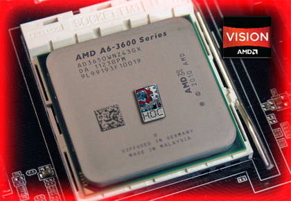
The series has three members, but initially only that A6-3650 will be available. The quad-core processor is clocked at 2,6 GHz and consumes up to 100 watts. This is followed by the A6-3600 - 2,4 / 2,1GHz (Turbo Core), also equipped with four cores. It can be seen from the APU numbering (ending in xx00) that its power demand is below 65 watts. In the smallest copy, the engineers deactivated a processor core, but applied no other change compared to the A6-3600. All three APUs feature the HD 6530D, in which 320 shaders have been activated.

The tip of the iceberg: A8 and A6 series
AMD A8 Series - The Upper Housing


AMD A8-3850 APU top and bottom
The most powerful Lynx APUs can be found here. The category currently relies on two models, but the A8-3870 “Black Edition” will arrive later this year. The four processor cores of the A8-3850 run at 2,9 GHz, so it's no wonder that the 100 Watt power is hungry. The A8-3800 - 2.7/2.4GHz (Turbo Core) - does not only look promising at first glance in terms of consumption performance. The integrated GPU of the A8 series is the Radeon HD 6550D.


"Sumo" is unbeatable
Llano’s “Sumo” integrated graphics processor is a kind of Redwood reincarnation. The IGP was equipped with five 80-way shader arrays, 20 Gather4-compatible texturing channels, and two ROP blocks with eight blending units. The GPU, of course, uses system memory to store data, which the APU can access through the dual-channel memory controller. Envelope in advance, the performance of a controller that is buffalo in its category depends significantly on memory speed. Based on measurements from foreign test sites, it is advisable to use at least 1600MHz DDR3 memories, otherwise a significant slowdown can be expected. Like the Brazos platform, all vendor-independent technologies are supported: DirectX 11, OpenGL 4.1, OpenCL 1.1, OpenGL ES 2.0, WebGL, WebCL, DirectCompute 5.0.

And the UVD 3 media engine guarantees H.264 / AVC, MPEG-2/4, VC-1, DivX and Xvid video acceleration up to Ultra HD resolution. AMD saw fit to revive the Hybrid CrossFire concept, now called Dual Graphics. This means that discrete graphics cards defined next to the Llano IGP can be associated, adding up the speeds of the two. However, the function only works with a few controls, which are shown below. The PCI-E controller can handle a total of 24 bands, of which 16 are for an external video controller, 4 for the FCH, and four more for devices that require low latency and relatively high bandwidth, such as Ethernet.
Thank you, you can sit down, great.


The other side of the coin
The CPU cores, called the APU Husky, don’t have third-level cache, but engineers have increased the size of the L512 cache from 1 kilobytes to 2 megabyte, somewhat to make up for the shortfall. The cache size of L1 data and L1 instruction is 64-64 KB.

The structure of the architecture is very similar to the already obsolete K10 solutions. Each core consists of 35 million transistors, has an area of 9,7 mm2 and a typical consumption of 10-15 watts, which can be reduced to 2,5 watts when unloaded due to aggressive gating. The instruction sets include SSE1, SSE2, SSE3, SSE4A and all 3DNow! knows the extension. Given the history of the architecture, unsurprisingly, it does not support SSE 4.1 and 4.2.

The presence of TurboCore 2.0 is not a negligible factor. This feature even came with Thuban tiles. The method is able to greatly increase the clock speed of the processor cores only if the increased consumption does not exceed the maximum specified TDP limit. Using a specific example for ease of understanding: if the IGP is fully loaded, the CPU clock cannot be raised, but if only the UVD engine is loaded - which has negligible power consumption - TurboCore 2.0 can significantly increase the Husky core clock so that the increased consumption still fits within the predefined TDP frame. This can mean up to 35 MHz extra speed for 900-watt mobile versions. It’s also important to mention here that TurboCore 2.0 only applies to processor cores, not to IGP anymore.
Closely related to this is the improved energy management, which is now able to completely disconnect components that are not in use, thus significantly reducing chip consumption.

{jospagebreak_scroll title = A75 and A55 FCH, motherboards}
It is worth mentioning the unit called FCH, or Fusion Controller Hub, which can practically be thought of as a kind of southern bridge. Two versions of this will be available for the Sabine mobile platform, one is the A70M and the other is the A60M. There is only one difference between the two: the A70M offers four USB 3.0 ports, while the A60M does not offer any, only 2.0 is available here. However, we are currently more interested in the desktop region, i.e. Lynx, there are also two FCHs available here, the A75 and the A55 Fusion Controller Hub.

The launch of the A75 FCH (Hudson D3) and A55 (Hudson D2) at AMD will also bring Intel to the lineup already in the world of chipsets. The north-south bridge pair has been discontinued, replaced by a single tile called Fusion Controller Hub at AMD. This allowed the PCI Express controller to move into the APU, just like with today’s Intel processors, so a northern bridge no longer made sense. A tile is always better for both if it does not involve a step back in service. Lower manufacturing costs, less heat generation, simpler construction, in a word, the arrival of FCHs is a joyous fact on the Socket FM1 platform. As shown in the figure, the point has been added to the APU, the A75 FCH only transmits four additional 1-wire PCI Express threads (500 MB / s) in this regard. Some of the other content is standard: HD audio, PCI controller, infrared port, six SATA 3.0 ports (6 Gbps) with AMD Raid Expert and FIS Based switching support, four USB 3.0 ports, ten USB 2.0 ports, and two pieces of USB 1.1. What’s a little more interesting is the presence of the Integrated Display DAC (VGA), SD Controller, APU Fan Control via SB-TSI, and Integrated Clock Gen (which also includes the clock generator), which are also housed in the FCH.

As you can see, the A55 does not differ much from the A75, the only difference is that FIS Based Switching for the SATA ports and USB 3.0 are not supported. The latter is not a lucky move, since today a motherboard without USB 3.0 is almost unsellable from the manufacturers' point of view, that's how it was marketed. For this reason, an external chip is again required for USB 3.0, which means that the combined cost of the A55 and the additional chip may already exceed that of the A75. So it's no wonder that at the moment we can't even find a model based on the A55 FCH at ASUS, while GIGABYTE also offers only five models, with one thing highlighted in red letters: "The motherboard has the features and price of the A55, but the A75 Includes FCH due to unavailability of A55”. – Well, this is another and very clear explanation of the situation.
Motherboards for Llano
Of course, the "pro" was also provided by our partners this time, a GA-A75-UD4H from GIGABYTE, and an F1A75-V Pro from ASUS. Both models compete in the HUF 30 price category, so they are practically competitors. Now we get to know them a little more closely.
Gigabyte ga-a75-ud4h

Following the average construction, the 30,5 × 24,4 cm ATX standard model comes to life externally according to the already proven GIGABYTE recipe. The components are on the blue PCB, including the Socket FM1 socket, because if it is a Llano, we have to look for this socket in the field of the motherboard. From the outside, we don't see much difference compared to the AMx edition, the plastic frames have also remained, so we can use our existing AM2 (+) / AM3 (+) compatible cooler on this platform as well. The APU 8 + 2, while the memories operate in 1 phase, the modules have four busses with dual channel mode support with a maximum capacity of 64 GB.


In terms of clock speed, 1066, 1333, 1600, 1866 and 2400 (OC) MHz RAMs are supported. The motherboard is powered by a 24-pin and an 8-pin power connector from the power direction. The A75 FCH (Fusion Controller Hub) rests in the lower right corner, similar to Intel motherboards working with PCH. The controller is cooled by a flat but wide rib, which we have seen many times on other models. The area of the expansion rails is quite rich. Three of the short, i.e. × 1 PCE Express slots have been added to the PCB, while two of the full-width, × 16 versions are available.


Thus, in addition to CrossFireX, AMD Dual Graphics can also be used in the event that an A-series APU is added to the system, in other words, the IGP working in the APU and the discrete graphics card can be used for cooperation. For the sake of old, the engineers also placed two pieces of traditional PCI on the UD4H, so if we have some older card, we shouldn’t be embarrassed either. At the bottom are the standard pin terminals - Firewire, USB (On / Off charge), front panel - and on the side we get five SATA ports, each of which supports the 6 Gb / s standard. Let's look at the back section!


The offering starts with a combined PS / 2 and two pieces of USB 3.0, and then comes the unmissable video outputs, as we’re talking about an APU, so something has to get things calculated by the IGP. No worries, we get everything we need, in addition to the standard VGA (d-sub) and DVI, the two defining connectors of our time, native HDMI and DisplayPort, are also part of the palette, and even an optical audio output is included. not possible. This is followed by two USB 2.0, one FireWire and one eSATA (6 Gb / s), followed by the gigabit Ethernet port and two more USB 3.0. As usual, the line is closed by the analog audio outputs, otherwise an 8-channel Realtek ALC889 chip is responsible for the sound generation.

ASUS F1A75-V Pro


At ASUS, black has been the fashion in the upper category for some time, this model is also based on black printed circuit boards, but blue is also dominant. Of course, this board is also based on A75 FCH (Hudson D3), so there are many similarities in design compared to the GIGABYTE model. The size of the PCB is 30,5 × 24,4 cm, around the socket FM1 socket the already run-in Digi + VRM tops with a 6 + 2 phase design.


Four slots can be used for RAMs, the modules can have operating frequencies of 1066, 1333, 1600, 1866 and 2250 (OC) MHz, with a maximum usable amount of 64 GB. On the power supply, we will need a 24-pin and an 8-pin power connector for power supply. The temperature of the PWM area is monitored by a design blue rib that communicates with the flat rib on the A75 FCH using a thick, flattened heat pipe.


The range of expansion rails on the F1A75-V Pro is also very rich. We get three from a standard PCI slot, while two can be put to work from a × 1 PCI Express. Of course, the most attention is always given to the full-width, × 16 slots, two of which are placed in the same way as the UD4H. This also means that Dual Graphics can be used with the A-Series APU, and CrossFireX is not required. Below you will find the USB and front-pin pins on the motherboard, and the SATA connectors on the F1A75-V Pro are also in the usual place, seven in number.


Of these, six white ones come from the Hudson D3, even blue comes from the ASMedia controller. Four fan connectors have been added to the board, three of which have 4-pin, i.e. PWM, controls. ASUS TPU and EPU technologies can also be physically controlled from the PCB with sliders, located at the edge of the PCB, behind the RAM DIMMs. The tab already contains the next generation UEFI BIOS.

The back cover promises a similar offering as the GA-A75-UD4H. Here, too, the kit starts with a combined PS / 2 connector and continues with two USB 3.0, the first column, followed by optical audio output, native HDMI and DisplayPort. If that weren’t enough, of course, VGA and DVI output can also be used. These are followed by the eSATA (red) port that comes from the ASMedia controller and is standard 3.0. This column is closed by two more USB 3.0, in addition to which only the Realtek gigabit Ethernet controller RJ45 connector, two USB 2.0 and analog outputs remain, which also operate from a Realtek chip, the ALC892, supporting up to eight channels.


{jospagebreak_scroll title = Test Configurations, Settings, Tuning}

Test configurations


Catalyst Control Center has become the AMD Vision Engine Control Center
We have already presented the two Socket FM1 motherboards included in the test, and we have already tested the ASUS P8Z68-V Pro and ASUS Maximus 4 Extreme motherboards. As a repetition/replenishment, it is worth turning the page to "We tried: Intel Z68 and a large motherboard in the clamp", and the "Tried: ASUS Maximus IV Extreme + Core i7-2600k - the harvest season begins”. There is no model yet, and that is the ASUS M5A97 EVO. It’s a fresh, socket AM3 + socket board that relies on the AMD 970 / SB 950 chipset and is also prepared to receive the Bulldozer. The Phenom II X4 970 Black Edition processor has been placed in this motherboard.

The product has Dual Intelligent Processors 2 and Digi + VRM power supply, TPU and EPU as well as Auto tuning function can be used. The M5A97 EVO already has a graphical UEFI BIOS, with system management assisted by AI Suite II. Of course, it has all the capabilities in the field of hardware, ie it can be used in a CrossFireX configuration, and it also has SATA 6 Gb / s ports as well as USB 3.0 connectors.
Further details can be found on the official factory site: ASUS M5A97 EVO

AMD A6-3650 processor in the ASUS F1A75-V PRO motherboard and their settings:


AMD A6-3650 processor unloaded AMD A6-3650 processor loaded


ASUS F1A75-V PRO information and RAM settings


AMD Radeon HD 6530D information
A6-3650 APU Tuning
Since the A6-3650 APU has been with us for a long time, we also had the opportunity to see how willing the product is to tune. There are usually two options for overdriving, either to increase the multiplier or to increase the bus speed, or both. For AMD APUs, the situation is tricky. The multiplier is visible and adjustable in the motherboard BIOS. For the A6-3650, the factory multiplier is 26, which could be increased to 47 on the ASUS motherboard. If we save this nicely and restart the machine, we can immediately see an APU ticking at 4700 MHz without any other parameterization, no voltage increase. Do we believe this? Well not very… And if we start the CPU-Z, the 4700 MHz will return there, but if we do some tests, we can see that the performance has not changed a bit compared to the 2600 MHz clock. It is a bug, a mistake, however we beautify it. So the erroneous display should not deceive anyone, APUs are not multiplier-free, a multiplier higher than the default is only seemingly active, not in practice!


Since we cannot deal with the multiplier, we are left with machinating the bus speed. Yes, but the frequency of PCI Express cannot be fixed for Llano units either. This means that we cannot increase the speed of the bus mindlessly either, because the operation of the components (LAN, USB) operating on PCI Express fibers can quickly become unreliable. The situation is definitely better than in the case of Sandy Bridge CPUs, but you have to be prepared that a significant tuning will also require a serious voltage increase. We went from 100 MHz to 140 MHz with an APU base voltage of 1,56 V (we also increased another in the BIOS), the resulting 3640 MHz value was still stable, but we ran into problems above that. It should be added that this value was also only OK if we used a discrete graphics card, because in the case of the HD 6530D, even with +10 MHz tuning, the edge of the image immediately "hanged out of the monitor". In any case, we performed the measurements with 3640 MHz, which we also did with the base clock, to see how much + 1 GHz matters in the case of an APU.
Tuning the AMD A6-3650 processor in the ASUS F1A75-V PRO motherboard and their settings:


AMD A6-3650 tuned in unloaded condition AMD A6-3650 tuned in unloaded condition


ASUS F1A75-V PRO tuned RAM settings Multiplier error for Llano APUs
AMD A8-3850 processor in the GIGABYTE GA-A75-UD4H motherboard and their settings:


AMD A8-3850 processor unloaded AMD A8-3850 processor loaded


CPU-Z cache and motherboard information

GIGABYTE GA-A75-UD4H RAM settings


AMD Radeon HD 6550D information
AMD A8-3850 processor in the ASUS F1A75-V PRO motherboard and their settings:


AMD A8-3850 processor unloaded AMD A8-3850 processor loaded


ASUS F1A75-V PRO information and RAM settings
AMD Phenom II X4 970 Black Edition processor in the ASUS F1A75-V PRO motherboard and their settings (3500 MHz):


AMD Phenom II X4 970 Black Edition processor in the ASUS F1A75-V PRO motherboard and their settings (2900 MHz):


Intel Core i7-2600k processor in ASUS P8Z68-V PRO motherboard and their settings (2900 MHz):


Intel HD Graphics 3000 (partial) information
Intel Core i7-2600k processor in the ASUS Maximus 4 Extreme motherboard and their settings (3300 MHz):


{jospagebreak_scroll title = AIDA64 Memory Operations, Mass Storage Tests, Consumption, Warming}

AIDA64 Extreme Edition 1.80 memory speed measurement:


AMD A6-3650 APU (2600 MHz) + ASUS F1A75-V PRO AMD A6-3650 APU OC (3640 MHz) + ASUS F1A75-V PRO


AMD A8-3850 APU + GIGABYTE GA-A75-UD4H AMD A8-3850 APU + ASUS F1A75-V PRO


AMD Phenom II X4 970 BE 2,9 GHz + ASUS M5A97 EVO AMD Phenom II X4 970 BE 3,5 GHz + ASUS M5A97 EVO


Core i7-2600k 2,9 GHz 4/4 + ASUS P8Z68-V PRO Core i7-2600k 3,3 GHz 2/4 + ASUS Maximus 4E
AIDA64 cache speed test (read test suite):


AMD A8-3850 APU + GIGABYTE GA-A75-UD4H AMD A8-3850 APU + ASUS F1A75-V PRO


Core i7-2600k 2,9 GHz 4/4 + ASUS P8Z68-V PRO Core i7-2600k 3,3 GHz 2/4 + ASUS Maximus 4E

AMD Phenom II X4 970 BE 3,5 GHz + ASUS M5A97 EVO AMD A6-3650 APU + ASUS F1A75-V PRO
Consumption and warming:

Of course, we couldn’t go past the configurations without examining them in terms of consumption as well. In the first step, we compared systems with graphics integrated into the processor, which meant the A8-3850 with two motherboards, and the Core i7-2600k limited to 4 cores and 4 threads (with HT off, without Turbo Boost) on the ASUS P8Z68 -V PRO tab. The values were measured with our standard, simple plug-in wattmeter, so they can still be considered as indicative rather than laboratory, accurate measurements.

Thus, the two processors (even if they are not direct competitors to each other) can be compared on the same core number and clock, in both cases in the company of IGP. Well, there seem to be some sort of miracle with the K12, as we saw lower values on the A3-11-based systems than on the Intel Sandy Bridge flagship, even when unloaded, under Blu-ray playback and 8Dmark3850. This is probably due to the Radeon HD 6550D, which is energy efficient, and compared to the fact that it is much stronger on paper than Intel's HD Graphics 3000, it doesn't eat much more than FurMark, the difference is only 15 -16 watts.
The A6-3650 APU on paper is in the same 100-watt TDP class as the A8-3850, yet we expected to encounter slightly more subdued values than our big brother, the A8-3850. This conjecture was nicely confirmed, as we measured the lowest values in all respects with the A6-3650. The difference was around 10 watts on average compared to the larger Llano, but in the case of Furmark, for example, we found an even bigger difference.

The line of positive surprises continued even when a Radeon HD 6790 was inserted into the system as a discrete graphics card - at which point, of course, the IGPs became inactive. Unloaded, the Llano was able to maintain its lead and also ticked off the Phenom II X4 970 BE, as well as the Core i7-2600k, which had joined in the meantime. With an AIDA64 load, the order of the world is already being restored, here the CPU cores are receiving a rough load, and this is already reflected in the measured values. There is so much good news that seeing the Phenom II, I managed to carve 12-13 watts at the same clock. Interestingly, for Blu-ray playback, the 3,3k set to 2600 GHz with the M4E board ran quite a bit, while the same CPU at 2,9 GHz with + 2 cores consumed the least in the P8Z68-V Pro. Of course, the focus is on the A8-3850, which doesn’t produce bad values here either, if not to a huge extent, but it has managed to move forward over the previous generation, even though we know that there is virtually no difference in architecture. Under 3DMark11, the field was pretty much the same, surprisingly, the quad-core Phenom banging at 2,9 GHz won that number. Under FurMark, the A8-3850 shines again, it reaches with the least energy, followed by the 2,9k working at 2600 GHz. It’s no big surprise that the X4 970 BE absorbs most of the network.
After measuring the consumption with IGP, we expected that Radeon HD 6790 would also demonstrate less energy hunger. This is also the case, as it eats significantly less than the A8-3850 in this test as well. This measurement also showed that tuning and voltage boosting have a serious price on the altar of consumption, as at 3640 MHz it jumped to the forefront everywhere except FurMark and Blu-ray, meaning it consumed most of its energy.

AMD A8-3850 APU

AMD A8-3850 APU
As you can see, the support of the A8-3850 is not completely perfect yet (we got 9 degrees for the minimum value), but it seems that the factory cooler added to the processor, resting in the box, was able to cope with the task entrusted without any problems, its use did not result in any instability, without a hitch, and compared to that he did his job quite softly.

A8-3850 + Radeon HD 6550D
The IGP sensor also transmitted surprisingly low values to the MSI Afterburner, according to the program, the idle Radeon HD6550D warmed to 11 degrees and then warmed up to 43 degrees under load. If the latter value is correct, it is to be commended again, especially by using the simple factory cooler supplied with the processor during the test.

AMD A6-3650 APU

AMD A6-3650 APU

AMD A6-3650 APU + Radeon HD 6530D
For the A6-3650, we already attached our usual Scythe cooler to the APU, since this unit came in "tray form". The AIDA64 loading and measurement was carried out at the base clock during monitoring. Accordingly, the Scythe monster handled it without any problems, the APU heated up to a maximum of 38 degrees, if we can believe the reading. MSI Afterburner was already in more trouble with the Radeon HD 6530D IGP, let's just say that we will return to the temperature data in a later test.
{jospagebreak_scroll title = Processor Power Measurements}
Results of our measurements:

Processor tests:
Synthetic and other measurements

The SuperPi is a relatively old and not very modern measuring program, it can handle only one thread, however, it is still very popular today, so it is not usually missed by us. This program has been a specialty of Intel processors for many years, AMD models usually come from a decent distance, and it’s no different now. Even with a run of 1M, there are huge differences, so it’s no wonder the field breaks apart at the biggest 32M calculation. The Sandy Bridge models fight in a separate league, but more interesting is the relationship between the Phenom II and the A8-3850 APU at the same clock, as in the longer term the APU was able to bring more than 1 minute to its predecessor. Obviously, the situation is different on the original clock of the 970 BE.
Because the A6-3650 is virtually identical in design to the A8-3850, it is expected to be as much slower than the 300 MHz clock difference in tests of processor power. We can also see the first signs of this in connection with the Super Pi, the disadvantage of the 1M calculation is about 2 seconds compared to the big brother. The same goes for the 32M, in proportions, of course. Tuning, on the other hand, gave wings to the A6 and immediately made it the fastest APU, which of course wasn’t a big surprise because of the 3640 MHz clock. Interestingly, while not for the 1M measurement, the 32M was able to roll down the Phenom II already running at 3,5 GHz.

WPrime, like the SuperPi, is a calculation meter, but it can now take advantage of running multiple cores or running multiple threads. You can see that, the field jumped a little more, and to my surprise, the Phenom II 970 BE took the lead at 3500 MHz. He is followed by 2,9k with 2600 GHz, four cores. The A8-3850 APU’s performance can be enjoyed so much that it was able to beat the Phenom again at the same clock, even if not by a big difference.
Switching to wPrime, we can report the same trend as we saw in Super Pi. At the base clock signal, it is slightly slower than the A8-3850, but when tuning it jumps significantly forward, so if consumption is not so important for us, it is worth setting a serious clock increase for our APU.

The Fritz 12 is no stranger to us either, which is a chess program with a built-in measurement module that shows how many times faster a given central unit is than a 1 GHz Pentium III using a multiplier in addition to a score. This number also brought a 4k victory over 4 cores and 2600 threads, but the 3,5 GHz Phenom also kept up with it for a long time. The A8-3850 once again brings the form that it runs better clock-to-clock than the Phenom II, but the difference isn’t significant right now.
In Fritz 12, at baseline, the A6-3650 was just able to beat the 3k setting that emulated the i2120-2600, but lagged significantly behind the others, thanks to the 2600 MHz operating frequency. The tuning changes the position of a horse kick and flies the Llano child all the way to the bottom rung of the podium.

A utility called TrueCrpyt can be used to calculate AES encryption. Well, since the 2600k hardware supports this kind of operation, it came as no surprise that it stepped down from AMD. Behind it runs the 970 Black Edition, which runs at its original clock speed, which the APU was once again able to beat at the same clock speed, so it increasingly seems that minimal performance gains can be expected in terms of CPU power as well.
Because AMD APUs don’t have hardware AES support either (unlike Sandy Bridge), they can only rely on cores and clock speed. So it’s not surprising the last place in the A6-3650, but the scale is all the more so. In addition, this APU barely accelerated due to tuning, so there is a reasonable suspicion that your relationship with this program was not cloudless.

In the final version of AIDA64 1.8 we ran the usual measurements, the results are very diverse. Under Quenn, the APU only has a chance against the Phenom working at the same clock, but it also manages to beat it, it can be slowly said that in the usual way. In Photoworxx the stunt fails, the A8-3850 is in last place. AMD units show surprising power in Hash, the 2k shortened to 2600 cores and HT lags ugly behind, but even the 4-core setting gets knocked out by AMDs, which is then won by the Phenom II X4 BE, so the APU slips behind. There are no huge differences under VP8 either, the good news is that Llano’s child can get over Phenomon here too. The FPU Julia shows the strength of the Intel CPUs, followed by the Phenom at the original clock speed, but at the same frequency, the APU wins again, adding that the difference is minimal.
On the base clock, the A6-3650 also brings logical scores on AIDA64 measurements, both relative to its big brother and the other units. Tuning throws a lot at its results in most places, with Queen at the forefront, for example, but it also emerges as the fastest AMD unit in Photoworxx. The only place where the power of overdrive was not clear was the FPU Julia module.

Rendering, encoding, compression

The Cinebench R10 is an older version of the popular rendering application, but is still perfect for measurement today. In the first round, we examined single-fiber work, followed by measurements using all fibers. The architectural advantage of Intel CPUs can be well traced here, there is still room for improvement for AMD, maybe the Bulldozer. However, it also looks nice that the K12 was able to accelerate somewhat compared to its predecessor. The setting captured on two cores (trying to mimic the Core i3-2120) in the second test with the HT is able to defeat the native 2900-core Phenom set at 4 MHz. The former can just be beaten by the A8-3850, which is good news compared to the Phenom, but the gentleman here is the Sandy Bridge.
Like many test programs, the Cinebench R10 presents the 6 MHz disadvantage of the A3650-300 APU compared to the A8-3850. Unfortunately, this results in him being the slowest member of the field in this number. Tuning helps a lot in your position, using a core to fly all the way to third place, while working with all the cores you also manage to get on the podium.

Cinbench R11.5 is the latest version where measurement is done using all cores and fibers. On 4 cores, the 2600k and Phenom 970 BE will step, while at the latter 2,9 GHz it will again only get out of the APU. The Sandy Bridge CPUs captured by the two cores bleed against all their opponents, in vain for Hyper-Threading. Another good point for Llano, he managed to improve a bit here as well.
The Cinebench R11.5 shows the same phenomenon as its predecessor. At its original 2600 MHz clock speed, the A6-3650 is at the very end of the field, unable to compete with the others, while the 3640 MHz frequency once again flies the unit to third place. It also shows how important it would be for both AMD and customers to be able to scale Llano models to higher clock speeds.

In the Photoshop test, the time taken to complete a finished script (calendar builder) was measured using a stopwatch, and then the results were summarized. Of course, the less time the operation took, the faster the CPU was considered. This race also favors Intel, with the fresh APU although it wins over Phenom, the difference is in tenths, meaning it’s almost insignificant.
Adobe Photoshop programs have not been a favorite of AMD processors for a long time, as can be seen in our CS4 script runtime measurement. The A6-3650 is roughly 2,5 seconds behind the A8, doing so at 300 MHz minus. Overcoming, he managed to fall in front of the family member and the upcoming Phenom, but he was already 0,2 out of the tuned version of it. There is no way to squeeze Intel CPUs.

Video conversion is an important part of our test, which was again measured using Cyberlink MediaEspresso by transcoding a 1080i resolution raw material recorded with a JVC HD camera into various formats without using GPU acceleration, in other words relying solely on processor power. The program is able to take advantage of the capabilities inherent in multi-core CPUs, but it does not despise the high clock signal either. It’s clear that each format is nicely able to shuffle the cards, but in most places the 2600k is the gentleman with 4 cores. The bottom line for the A8-3850 is that it managed to beat its Phenom counterpart running at the same clock each time, with a bigger or smaller difference.
Video conversion capabilities were tested in this test using CPU power only. Here, too, the A6-3650's performance showed an expected picture, meaning that it would be a few seconds behind the 3850, which would have made it different. The OC still brought a lot to the kitchen, so the Phenom II X4 was in serious competition with 3,5 GHz. The disadvantage of i3,3-3 emulation at 2120 GHz is only one second in two cases, while it clearly beats it in two cases.

With Winarr, we have reached the end of tests that specifically evaluate CPU power. The program takes advantage of multi-threaded instruction execution, so the 2600/4k 4/2 stunt is no surprise, with a 4/970 setting, the Phenom 3,5 BE is wedged between 2,9 GHz and XNUMX GHz. The current strongest representative of the Llano platform failed this time, which he did so many times, i.e. this time he could not beat the Phenom on the same frequency.
Winrar has a very simple and fast measurement module. "You don't have to take your word for it", but due to tradition, he didn't miss out this time either. The numbers show the usual picture. At the base clock, the A6-3650 is at the back, while with + 1 GHz it moves up to third place. It is interesting to see that although it has a 140 MHz advantage over the overclocked Phenom II X4, its performance against it varies, sometimes it wins and sometimes it loses.

{jospagebreak_scroll title = Measurements with Radeon HD 6850 Discrete Graphics}

3D measurements with HD 6790

The Vantage Intel CPU showed superiority in terms of Performance score, with them only the Phenom 970 BE was able to keep up somewhat, but he was also only at 3500 MHz. The setting working at 2900 MHz and the APU results are very close to each other, practically the same. The CPU score provides slightly more information about the power of the CPUs. The trend is similar, unfortunately the APU production this time lags behind the Phenome set to the same clock, although the difference is negligible here as well.
In 3DMark Vantage, the A6-3650 is not far behind the A8-3850 in terms of Performance score, here the 300 MHz disadvantage is not so much a cut, but it is just a measurement program, the more important numbers will be in each game we will see, i.e., the FPS values.

3DMark11 also brought Intel processors to victory, but more importantly, what the new APU shows. It couldn’t stifle competition from the manufacturer (though the differences aren’t big here either), but with the Phenom II X4, it successfully picked up the glove not only at the same operating frequency, but also against the original clock running at 600 MHz extra.
The thing paints a similar picture to that of the Vantage. The field is close enough to each other, and we can certainly report a few oddities. The first is that for some reason the tuned measurement yielded fewer results than the base clock test. The latter was able to crush the tuned Phenom, and he was just behind his big brother. Although there is no big difference, it has not been possible to get there with Intel processors either.

Under Unigine Heaven Benchmark 2.5, the story is pretty VGA-limited, but there are small differences in the scores that meant the A8-3850 APU could be a hair's breadth faster on the same frequency than the Phenom II X4 970 Black Edition, which is another strigula, but the biggest force this time around was Intel processors.
While running Heaven, we again found that tuning did not work. Either Catalyst 11.9 improved back to 11.6b or there was something wrong with OC, not sure. What is certain is that the program ran stably, without any problems. In Heaven, the graphics card is loaded so much that the individual central units can only have a minimal influence on the numbers, as we can see in the graph above.

We will move on to the games below. Well, Crysis 2 already proved to be a VGA limit in DX9, but we measured it with similar parameters, because we were curious to see if we could benefit from different CPUs with real game settings, as a CPU around 30 HUF and a similarly priced CPU The AMD Radeon HD 000 doesn’t seem like a bad pairing, and with such a card you can target 6790 × 1680 resolution, but even FULL HD. Crysis 1050 doesn’t spare VGAs, so there was no difference in FULL HD anymore, at lower resolutions, Intel CPUs were able to show 2 FPS advantage.
Unfortunately, we could not change the measurement parameters, so in connection with Crysis 2, the VGA limit came into force again. We were able to add 1 FPS plus to the tuning and newer Catalyst bill.

In Dirt3, the field has already begun to break down a bit. On 4 cores, the 2600k is ahead at 2900 MHz, but the A8-3850 APU lags only 1 FPS, and with a 2600k 3,3 GHz 2/4 setting, it knew the same FPS. It is also encouraging that it can show a 2-3 frame advantage over Phenom, let’s say it’s a mystery why the Phenom was slower at 3,5 GHz than at 2,9 GHz.
Dirt3 has already separated the riders better. At the base clock, the A6-3650 was 2 and 1 FPS behind the larger APU, the Phenom was running at the same resolution at the lower resolution, while it was already knocked down on the FULL HD. Interestingly, the tuning did not work for either the Phenom II X4 970 BE or the A6-3650. Intel CPUs also win that number.

Far Cry2 also made a difference, the scheme is similar to that of Dirt3. The 2600k with four cores and four strands in the front, the Llano APU tied with the 2600k in the core behind it, and the Phenom in the back, so the A8-3850 was able to win its in-house battle now, which can be rejoiced again.
At Far Cry2, with the exception of Sandy Brige running at 2,9 GHz, the field is pretty tight, the speeds of the two APUs are almost the same, while the Phenom is crushed. For some reason, the overclocked clocks were not successful here either, bringing either the same or fewer FPS.

Under Hawx2, the field isn’t overly torn, but the recipe still remains. In an attempt to mimic the Core i3-2120, the K12 runs the same setting, which treats Phenom again, if only by 1-2 FPS. In summary, the K12-based A8-3850 was able to accelerate slightly compared to the Phenom II, which isn’t really much, but more than anything, and it’s worth every little FPS treasure.
The values of Hawx2 are also pretty much the same. It appears that on the base clock signal, the A6-3650 slides to the rear at both resolutions, presumably the clock signal is tilted. Tuning here helps a little, but not nearly as much as we would have expected. Interestingly, it mattered more at the higher resolution. In 1680 × 1050 he managed to catch the tuned Phenom, but while he still lagged behind the others. Switching to FULL HD, they managed to beat at least the Phenoms, lagging behind the A8 and Sandy Bridge jackets by 1 and 2 FPS, respectively.

{jospagebreak_scroll title = Tests with Integrated Graphics}

Measurements related to integrated graphics:
We arrived at the most exciting stage of the Llano test, where we scrutinized the capabilities of the Radeon HD 8D rumbling in the A3850-6550. The situation is not entirely fair, as the strongest APU competes in the category of around 30 HUF, while the Core i000-7k costs more than twice as much, which is now interesting from the point of view of the stronger Intel HD Graphics 2600 in this process. student IGP works, while Sandy Bridge units available in price category A3000-8 are available with HD 3850 IGP. However, as soon as we see the results, the fact that the Radeon HD 2000D almost doesn’t care which Intel IGP you have to face will pretty much be outlined.
We’ve arrived for measurements related to integrated graphics, now we’ll see what the Radeon HD 6530D is capable of against its big brother, the HD 6550D and the Intel HD Graphics 3000. Of course, on a logical basis, it can be deduced what kind of picture the thing will paint, but it never hurts to know the specific numbers. Measurements were first performed with the standard 1600 MHz RAM clock signal and the then Catalyst. We then installed the latest WHQL driver available and repeated the tests. Finally, we increased the frequency of the RAM to 1866 MHz, and so we did a series.

In 3DMark Vantage, the Radeon HD 6550D instantly gives you a taste of what wood it was carved from. Even the Sandy Bridge CPU cores in the CPU score can save Intel’s IGP, but the Performance result and GPU score give a clear signal that this fight will bring a close fight in the rarest of cases. The Radeon 6650D received about twice as many scores as the HD Graphics 3000.
Vantage under the GPU and P score, which is now interesting to us. As expected, the HD 6530D is wedged somewhere halfway between the HD 6550D and the HD 3000, and for sure, this Radeon is much stronger than the HD 3000.

In 3DMark11, due to the basic requirement of DirectX11 (Intel's IGP is lagging behind due to DX10.1, too) we could not include HD Graphics 3000, the HD 6790 jumped in its place. Obviously, the 6550D IGP could not compete with it, but setting proportions is not useless for the result. Under the Performance profile, the HD 6790 has a score of ~ 2,8 times higher. Considering that the HD 6790 is a $ 30 discrete controller and the HD000D is a unit integrated into a processor, and the entire package costs $ 6550, this is not a bad result for IGP.
In 3DMark11, due to the basic requirement of DirectX11 (Intel's IGP is lagging behind due to DX10.1, too) we could not include HD Graphics 3000, the HD 6790 jumped in instead. His score is just an interesting value, the focus is on the two IGPs. The HD 6530D is 30-35% slower than its brother. The newer Catalyst had a lesser role, the faster a memory more.

Video conversion measurements had previously been performed using only the CPU cores, of course the GPU acceleration test could not be missed either. The 2600k was measured at 2,9 GHz with the 4 core / 4 fiber setting paired with the built-in IGP, while the other configuration was paired with the HD 6790. Converting to DivX seems to be a big favorite of the Intel HD Graphics 3000 (in fact, the Intel Quick Sync Video dedicated decoder unit integrated into the processor plays a huge role in this), as it has beaten the Radeons terribly. The good news is that the A8-3850 comes in second with the HD6550D, which was able to run more efficiently than the Phenom + 6790 and 2600k + 6790 pairs. HD Graphics 3000 also takes pride in WMV encoding. For some reason, the 6550D isn’t so bright here and slips to the end of the field. Unfortunately, this format has been ported to both m2ts and h.264 formats, we have a feeling that software support for Llan is not yet a perfect fix and performance improvement that can be imagined in the future.
In the field of video coding, the 6530D produced interesting things, perhaps after the previous measurement as well as carving out software support. With DivX and wmv encoding, we don't see any signs of that yet, although the former is faster than the HD 6790 and only gets out of the 6550D and HD 3000, respectively, while the latter suddenly gets to last place. The surprise comes with m2ts and h.264 encoding. Converting to the PS3 took almost half as long as the HD 6550D, but it could take almost 264 seconds for the h.70 as well. In vain, there is a great need for continuous development of applications and drivers in this area.

Under Alien versus Predator, we looked at how much the game can be played with the Radeon IGP. The benchmark application is a very tough scene using DX11, of course for the playable level, tessellation and other extras should definitely be turned off for an IGP. With medium detail, at lower resolutions, you can reach the limit of what you can still play with, but overall, AvP is a big challenge for the Radeon HD6550D.
In AvP, due to the DX11, only the IGPs of the two APUs could compete with each other. The disadvantage of the smaller Radeon is 10-25% depending on the resolution, the newer drive and the faster memory couldn't really speed it up. In any case, at low resolution, the game remained close to playability even with the 6530D.

In Battlefield: Bad Company 2, Intel HD Graphics 3000 is back, of course he could only do the tasks with DX10.1 knowledge. As a result, it doesn't disturb much water, as the Radeon HD 6550D is much stronger at all resolutions, with a high setting at 1280 × 1024, it stays close to the playable level. At 1680 × 1050, it already slides thickly below 30 FPS, but that can't be blamed on him, since we're talking about an integrated unit that runs a serious FPS with just high quality and resolution, just look at the HD 3000's 13 FPS.
At Bad Company 2, the HD Graphics 3000 may have been back, though in its case, the DX11 parts were omitted. With the Intel solution, the HD 6530D is clearly faster, lagging behind the 6550D by 27-36-35%. With the smaller Radeon, this game also seems to play only at the lowest resolution, unfortunately. It also includes the fact that IGP couldn’t really profit from either the newer drive or the faster memory.

During Crysis 2, despite the DX9 mode, we expected the IGPs to fall, but this measurement was certainly good to demonstrate the difference between Intel’s current strongest and AMD’s current strongest IGPs. While none of these settings can produce a playable level, it is clear that Radeon is much stronger than its opponent.
For Crysis 2, we guessed it was going to be a big bite for unfortunate IGPs, but interestingly, we did the measurements with it, where we then saw a miracle on the Radeon HD 6530D. Although it was even more powerful at the lowest resolution, in 1280 × 1024 it was already able to catch up with the Catalyst 11.9, and with 1866 MHz RAM. We can see the same at the highest resolution. Unfortunately, this has not changed the fact that this game can provide a somewhat continuous image with IGP at a maximum of 1024 × 768, but it would be a fault to blame any integrated unit for this.

Using the Dirt3 High profile, the GPUs did quite well, producing even the Intel IGP at the lowest resolution, and the HD 6550D was able to squeeze out 50 FPS. As the resolution increases, the HD 3000 runs out of power, but the HD 6550D lasts all the time, even at 1680 × 1050 it was able to fly the Dirt30 above 3 FPS in High quality, which is a brilliant production from an APU.
In Dirt3, it was a little surprising the weak performance of the HD 6530D, where it was only able to get ahead of the HD Graphics 3000 with a few FPS. Keep in mind, though, that the Radeon is a DX11-capable model, while the core in Sandy Bridge can only run in DX10.1 mode. However, in this title it is also significantly lower than the big brother, the difference is 12-10-9 FPS, which means 31-35-39%. The fresh drive and faster RAM couldn’t improve the situation either.

From what I’ve seen so far, it wasn’t surprising that Far Cry 2 also brought the dominance of Radeon, which was able to stay there all the way to the 30 FPS dream limit and well above it at lower resolutions, while HD Graphics 3000 is no longer at 1024 × 768. you can take this game that is already quite old. If our future machine gets an A8-3850 APU, we can count on not having to give up Far Cry 2 if we want to play.
Far Cry 2 is not today's chicken anymore, it was run in DX10 mode. Here, the 6530D significantly outperformed Intel's solution, but the "respect" for the 6550D was also shown, which can be called a power difference. The difference of 10-8-7 FPS was quite a lot, in percentage 27-28-30%. The fresh driver and 1866 MHz were also ineffective here.

We arrived at the last member of the 28 charts with HawX 2. This combat aircraft simulator is a very well-optimized, modern software, as evidenced by the fact that even with the High profile, all IGPs could play levels at all resolutions. The HD 3000 is close enough to the Radeon HD 6550D based on FPS, but this is only possible because it ran the benchmark in DX9 mode, while the 6550D used its DX11 knowledge and still had 37 FPS of its own. to squeeze out at 1680 × 1050. Bravo A8-3850 APU!
Our concluding title is Hawx 2, in connection with which it should be noted again that the Intel HD Graphics 3000 again ran the benchmark in a different way than the Radeons, only in DX9, which is clearly reflected in the results. The Radeons worked with DX11, tessellation, and they still stood the mud nicely, the HD 6530D, which could put 1680 FPS on the table even at 1050 × 29. However, Catalyst showed no increase in performance, and we could also write a maximum of 1 FPS on the faster memory bill. The lag behind the HD 6550D is 28-30 percent.
{jospagebreak_scroll title = Summary, Opinion}
Summary, opinion - A8-3850 APU

Once again, we have passed a terribly long test, the Llano platform and the AMD A8-3850 APU gave up the lesson properly, as we had to examine many things, which we tried to match with the available devices. With the release of this family, a long era at AMD has come to an end, and the Fusion era actually begins. In terms of processor cores, these APUs cannot be considered completely new, as they are reworked Stars cores, despite the K12 name. This was also shown in our processor power tests, but luckily the "revised" rating also appeared in the results. The A8-3850 is the top of the current range, it includes the most powerful graphics controller, the Radeon HD 6550D, with a clock speed of 2900 MHz, which cannot be increased with Turbo Core, because this model does not include this service.

To make a comparison with its predecessor, we used a Phenom II X4 970 Black Edition processor that was also measured at its original 3500 MHz clock speed as well as at 2900 MHz frequency, which is the same as the A8-3850 clock signal. In the vast majority of CPU measurements, we found that APU performance improved compared to Phenom II, sometimes to a greater extent, several times more modestly, but there was a clear improvement. This development can also be said for 3D applications and games, 1-2 FPS plus was able to present the novelty. Related to this is a further positive that overall consumption has also declined somewhat, with the A8-3850 making significant progress, especially when unloaded, and all of these changes can all contribute to success.

Sure, as a CPU, we didn’t expect too much from this model, as we knew it wasn’t yet representative of the new architecture, but it seems AMD did what it could. Llano’s real weapon, of course, is not this, but the use of an integrated, Redwood-based graphics core, which has proven to be a great pairing with the redesigned Stars cores. It is true that with the A8-3850 only the Radeon HD 6550D showed its capabilities, but everyone could see from the results that we have never encountered integrated graphics representing such power, and that this was finally achieved in a heterogeneously programmable chip, special joy and very encouraging for the future. We are living in an age of high degree of integration, and AMD has entered the market with an efficient product. The area of discrete video cards is shrinking, and for a significant portion of customers, the computing power that an HD 6550D, for example, can provide is sufficient.

With the advent of APUs, there is no need to purchase a separate graphics card, if you don't need a lot of power, then with an APU, an FM1 socket motherboard and some memory, we've already laid the foundation for our computer. Of course, AMD also meant those who want to move beyond the HD 6550D level later. It goes without saying that a discrete card can be used on the motherboard with the help of the PCI Express bus, but with AMD Dual Graphics we can ensure that the GPU dormant in the APU does not lie flat, but the two hardware work together, thus increasing the combined power. 3D performance. All you need to do is buy an A-Series APU and the right type of discrete Radeon. The former can be an A8 model with an HD 6650D, or an A6 HD 6530, the point is to associate one of these with the Radeon HD 6670/6570/6450, and Dual Graphics can already be activated, which also gives birth to new model names, all in the the easiest way to illustrate this is with the table below.

The performance of IGP can therefore be significantly increased with little effort and a little caution. Of course, we can also use a much more powerful discrete card, such as a Radeon HD 6970, but then the IGP dormant in the APU faces long periods of inactivity, thus losing the real advantage of the APU over the traditional processor. So AMD has also dreamed up the details carefully, launching the Lynx and Sabine platforms following safe steps, and if not as a CPU, but with processor-integrated graphics, it is currently the biggest force in both markets, significantly ahead of Intel HD Graphics 2000 and HD Graphics 3000 models. Of course, success with good hardware is far from certain, a lot depends on the price. In recent years, we have become accustomed to AMD not being disappointed in terms of purchase prices.
The strongest unit is the A8-3850, which is also included in the test, its boxed version can be purchased for less than 30 HUF for a gross 000 HUF, for which, in addition to the four native CPU cores, we also get the performance of a discrete card of about 29 HUF in IGP form. That’s why for the money, we can get roughly a Core i000-15 on the Intel line. During the measurement, we tried to simulate this CPU with 000k by turning off the 3 cores and setting the clock to 2120 MHz and leaving HT on, so except for the tertiary cache and HD 2600 we were able to perform the measurements with the same parameters. From these, it can be concluded that a Core i2-3300 - as a processor - is generally slightly more powerful than the A3000-3, but it also depends to a large extent on the specific application.

And when you compare the graphics solutions of the two processors, the APU’s Radeon HD 6550D also washes the Intel HD Graphics 2000 and 3000 off the track. In terms of consumption, the Sandy Bridge is still better in loaded conditions, so we need to consider before buying. If we need a modern and strong IGP, let’s clearly put our vote in favor of Fusion and choose the A8-3850. If IGP isn’t important, but you need CPU power instead, you can do better with the Core i3-2120, but you can also choose from quad-core Phenoms. Unfortunately, the A6-3650 did not come to us, but based on the available information, the purchase price of ~ 24 HUF seems a bit exaggerated compared to the 000 HUF amount of the A8-3850, based on the performance difference between the two models, some correction by AMD if the strength of the novelty depends a bit.
We’re curious to see what sales will show in a few months, and AMD doesn’t even stop the machine now. The appearance of the Bulldozer is imminent, which many expect a lot from. Either way, it’s so certain that an upgrade to the platform, codenamed Trinity, will arrive next year. This will already rely on Bulldozer-based CPU cores (modules), and IGP is rumored to be a Barts and Cayman merger, so there can be no question that the CPU performance and graphics power of APUs will continue to grow. , which will be the result of a brand new, modern architecture.

In the meantime, a good piece of advice for those enrolling in one of the desktop APU models. Because IGP is powered by system memory and the hunger for Radeon bandwidth is very high, we can benefit a lot from building fast DDR3 modules into our system. Feel free to forget the 1333 MHz RAMs if you want to be good, you should not give it below 1600 MHz. However, if you have a frame, preferring to get 1866 MHz or even faster memories, you’ll appreciate the little Radeon dormant in the APU. Fortunately, given current memory prices, this is no longer a million-dollar investment.

We looked at a lot of things about the A8-3850 and Llano, but at least that many topics were left out of the article. The reason for this was that the APU could only spend 2,5 days with us, so the time available and the number of additional hardware was finite. Regardless, we are confident that we have been able to answer the most important questions, and after reading this article, everyone can form an opinion about the AMD APU as well as make a purchase decision.

Of course, this test would not have been possible without the help of our partners. Both the GIGABYTE GA-A75-UD4H and the ASUS F1A75-V Pro did their job stably and reliably throughout. If we salivate through the graphs, we can see that to a very minimal extent the F1A75-V Pro was faster, but the differences are just as small as for Intel boards, because like Intel's PCH, AMD's FCH it has little to say about performance, as almost everything is housed in the CPU or APU, respectively. The equipment of the two models is very similar, if we are looking for a Socket FM30 motherboard with a Fusion construction intention of around 000 HUF, then we can confidently recommend either one.
Update: Summary and Opinion - A6-3650 APU
Slowly two months have passed since our article on the A8-3850 was published. A lot has happened since then, a lot has changed. Unfortunately, the output of Llano processors is still not real, few APUs are coming to market, and you should now share production lines with Bulldozer models. In addition, in terms of domestic conditions, it can be said that the forint is again terribly weak. As a result of these circumstances, what we described two months ago in terms of judgment and prices is unfortunately not all true today, as both the A8-3850 and A6-3650 have undergone significant price increases. At that time, the top model A8-3850 could be purchased for around HUF 29-30 thousand gross, today this amount has already increased to HUF 38, ie the product has become at least 000 percent more expensive. Now we are there that practically the A30-6 costs as much as two months ago for the big brother, ie 3650-28 thousand forints. Needless to say, this is of no use to customers or AMD at all. Let's look at the prices of competing Intel models! The 30 GHz Core i3,1-3 is included in the price with the A2100-6, ie it can be taken home for about 3650 forints. The Core i28-000, which is 200 MHz faster than this, ie in the test, simulated with 2600k at 3,3 GHz, can be found at an altitude of 3 forints. The fastest member of the family is the 2120 GHz Core i31-000, which costs 3,4 forints, this 3 MHz is no longer sure to be worth this extra money.

Speaking specifically of the A6-3650, it can be said that in the nine tests that tested processor power, it could only be faster than the Core i3-2120 emulation, while in the 6790D tests that included the HD 3, it lost six out of seven cases. and at the same time reaches a tie. Plus, the difference is often so definite that we feel it would look very similar to the Core i3-2100 in the price with it. Although we couldn’t make a completely accurate measurement because of the emulation, the at least good news is that it can already compete with these Sandy Bridge models in consumption, at least for us the numbers have shown this despite the 35 W higher TDP class. Overall, we still have the same opinion we had before about the A8-3850. It’s only worth buying an APU if we really need the Radeon graphics core inherent in it, and we’ll really use it, either on its own or as a Dual Graphics solution. The K12 + Radeon IGP pair is competitive against the Sandy Bridge + HD 2000/3000 pair, and in 3D power, AMD’s solution is an absolute winner, as is the level of technological sophistication. However, if you don’t need IGP, it’s not the best choice to invest in an APU, as it is stronger both within the manufacturer and on the Intel line. central unit we can get it for the same money.

In addition, we would add that the drive battle of Catalyst 11.6b vs. 11.9 yielded less than expected, many times we couldn’t even report a difference. Hopefully, the next Catalysts will still speed up on units dormant in APUs. The experience was similar with the 1866 MHz memories, we could add a little plus to their account, but let's not forget that the basic measurement was not with 1333 MHz but with 1600 MHz RAM, so the extra operating frequency is only 266 MHz, in addition, the delay increased from CL8 to CL9. The lesson of this is that there is no big difference between 1600 and 1866 MHz, compared to 1333 MHz we could probably have recorded more significant differences. I liked the A6-3650 as an APU overall, and if you want to build an integrated graphics, all-in-one machine that can even be played with, you can like the A8-3850, the A6-3650 we can also recommend. Looking at the product as a processor, as well as seeing the current inventory and current prices, we would rather say that we liked it and look forward to how it will develop in the coming months. We’re sure the next generation next year codenamed Trinity will sound bigger than these first series models.

AMD Plain
AMD A8-3850 APU
Gigabyte ga-a75-ud4h
ASUS F1A75-V Pro

AMD A8-3650 APU
I myself slowly put down the Llano lute and come to rest after the long test, but before that I have to thank med1on and Huskydog for their help in writing the article, and our partners can’t miss out on the thanks either:
The AMD A8-3850 APU and the GA-A75-UD4H motherboard a Domestic representation of GIGABYTE F1A75-V Pro, Maximus 4 Extreme, P8Z68-V Pro and M5A97 EVO motherboards Domestic representation of ASUS provided for our test, thank you!
The AMD A6-3650 APU is AMD provided us, thank you!
The article was written by: Zoltán Mihics (med1on) and Gábor Pintér (gabi123)
Thanks to the following sponsors for our permanent test components in this article:


